

Precision PCB manufacturing is essential for producing printed circuit boards that meet demanding electrical, mechanical, and assembly requirements. As electronic products become smaller and more complex, manufacturers must maintain tighter control over trace width, hole diameter, layer-to-layer alignment, and board dimensions. Even minor deviations can affect signal integrity, component placement, soldering quality, and final product reliability.
For OEMs, electronics manufacturers, and PCB procurement teams, understanding these accuracy factors is important when selecting a PCB supplier. Board precision does not depend on a single manufacturing process. Instead, it results from coordinated control across material selection, imaging, drilling, lamination, etching, and final inspection.
This article explains the key factors affecting PCB manufacturing accuracy and highlights what buyers should evaluate when sourcing custom precision PCBs.
1. Trace Width and Spacing: Controlling Circuit Pattern Accuracy
Trace width and spacing are fundamental parameters in precision PCB manufacturing. They determine how accurately copper circuits are formed and whether the finished board meets its electrical and design requirements.
As PCB designs become denser, maintaining consistent trace geometry becomes more challenging. Small deviations may change conductor resistance, affect impedance control, or reduce the clearance between adjacent circuits.
1.1 Factors Affecting Trace Width Accuracy
Several manufacturing variables influence the final trace width:
- PCB substrate and copper thickness: Different copper thicknesses require different etching conditions. Thicker copper generally requires greater control over the etching process.
- Photoresist imaging: Exposure energy, imaging resolution, and alignment affect how accurately circuit patterns transfer to the copper surface.
- Etching parameters: Etchant concentration, temperature, spray pressure, and processing time influence lateral copper removal.
- Line density: Fine-pitch designs and closely spaced traces require tighter process control to prevent shorts or open circuits.
Etching compensation is particularly important. Since chemical etching removes copper from exposed areas and can also affect trace sidewalls, manufacturers may need to adjust the artwork dimensions to achieve the required finished trace width.
1.2 Why Trace Width and Spacing Matter
Trace width affects electrical resistance and current-carrying capability. Trace spacing helps maintain electrical isolation and reduces the risk of short circuits.
For high-speed and high-frequency designs, trace geometry also influences characteristic impedance and signal behavior. Therefore, PCB manufacturers should evaluate trace width and spacing together with copper thickness, dielectric properties, stack-up design, and the electrical requirements of the application.
Buyers should provide clear design specifications, including minimum trace width, minimum spacing, copper weight, and any controlled-impedance requirements.
2. Hole Diameter and Drilling Accuracy
Hole accuracy is another important factor in precision PCB manufacturing. PCB holes support component mounting, mechanical installation, and electrical connections between conductive layers.
Depending on their functions, holes may be classified as plated through-holes (PTH), non-plated through-holes (NPTH), blind vias, or buried vias. Each type has different drilling, plating, and inspection requirements.
2.1 Factors That Affect Hole Diameter Accuracy
The finished hole diameter may differ from the original drill diameter because of several process variables:
- Drill bit diameter and condition: Tool wear, runout, and incorrect tool selection can affect hole dimensions.
- Drilling machine accuracy: Spindle stability, positioning accuracy, and machine calibration influence hole placement and geometry.
- Material characteristics: Glass fiber distribution, resin content, and substrate hardness affect drilling behavior.
- Copper plating thickness: For plated holes, the plating process reduces the available finished hole diameter.
- Deburring and desmear processes: Post-drilling treatments must be controlled to maintain hole quality and prepare the hole walls for reliable plating.
For example, the finished diameter of a plated through-hole is generally smaller than its mechanical drill diameter because copper is deposited on the hole wall.
2.2 Hole Position and Aspect Ratio
Hole accuracy involves more than diameter. Hole position, roundness, wall quality, and aspect ratio also influence PCB performance.
The aspect ratio is commonly expressed as the relationship between board thickness and hole diameter. A higher aspect ratio can make reliable plating more challenging because chemicals must reach the entire hole wall.
For multilayer boards, poor drilling or plating quality may lead to weak interconnections, incomplete copper coverage, or reliability issues during thermal cycling.
When evaluating a PCB supplier, buyers should confirm the required finished hole diameter, positional tolerance, board thickness, via structure, and plating specifications.
3. Layer-to-Layer Alignment: Maintaining Multilayer PCB Registration
Layer alignment, also known as layer registration, refers to how accurately individual PCB layers align during lamination. It is especially important for multilayer PCB manufacturing, where internal copper patterns must connect correctly through drilled and plated holes.
If internal layers shift during lamination, the final drilled holes may not align properly with their intended copper pads. This can reduce annular ring width, weaken electrical connections, or cause open circuits.
3.1 What Causes Layer Misalignment?
Several factors can contribute to registration errors:
Material expansion and contraction
PCB laminates expand and contract in response to temperature and moisture changes. Different materials may exhibit different dimensional changes during processing.
Lamination temperature and pressure
Uneven temperature distribution, pressure variation, or inconsistent curing conditions can cause dimensional instability during lamination.
Inner-layer imaging accuracy
Errors during inner-layer exposure, etching, and tooling can accumulate and affect the alignment of the finished stack-up.
Tooling and positioning systems
Pin registration, optical alignment, and automated positioning systems help control layer placement. Their accuracy and calibration directly affect registration quality.
3.2 Why Layer Alignment Is Important
Accurate registration helps maintain sufficient annular rings around drilled holes and ensures reliable connections between conductive layers.
It is particularly important for:
- High-density multilayer PCBs
- Fine-pitch component designs
- Boards with small via structures
- High-speed and high-frequency circuits
- Complex HDI PCB designs
Manufacturers can improve registration control through material characterization, compensation of inner-layer artwork, stable lamination processes, and appropriate alignment systems.
For buyers, it is useful to discuss layer count, stack-up structure, minimum annular ring requirements, via dimensions, and registration tolerances before production.
4. PCB Dimensional Tolerances: Maintaining Board Size and Geometry
PCB dimensional tolerance describes the acceptable variation between the specified design dimensions and the actual dimensions of the finished board.
It covers more than overall board length and width. Depending on the design, it may also include thickness, hole-to-edge distance, slot dimensions, cutouts, outline geometry, and component positioning references.
4.1 Factors Affecting PCB Dimensions
The final dimensions of a PCB can be influenced by several manufacturing stages:
- Laminate properties: Substrate materials have different coefficients of thermal expansion and dimensional stability.
- Thermal processing: Heating and cooling during lamination, solder mask curing, and other processes can cause expansion or contraction.
- Mechanical processing: Routing, punching, and V-cut operations affect the final board outline.
- Panelization: The arrangement of individual boards within a production panel can influence processing stability and material utilization.
- Moisture absorption: Certain laminate materials may change dimensions when exposed to moisture.
Dimensional stability becomes especially important for boards that must fit into precision enclosures or align with connectors, mounting holes, and mechanical components.
4.2 How to Specify Dimensional Tolerances
Procurement teams should avoid relying only on general statements such as “high dimensional accuracy.” Instead, they should define measurable requirements in the PCB drawings and manufacturing data.
Important specifications may include:
- Finished board length and width
- Board thickness and tolerance
- Hole diameter and positional tolerance
- Slot and cutout dimensions
- Edge-to-hole distance
- Board outline and profile requirements
- Flatness or warpage requirements, where applicable
The appropriate tolerance depends on the board design, material, thickness, manufacturing process, and assembly requirements. Tighter tolerances may require additional process controls and inspection, so they should be specified according to actual functional needs.
5. How PCB Manufacturing Processes Work Together to Improve Accuracy
PCB accuracy is not controlled by one isolated operation. It depends on how well each manufacturing stage supports the next.
The following processes have a direct influence on finished board precision:
| Manufacturing Process | Main Accuracy Concern | Typical Control Measures |
|---|---|---|
| Material preparation | Dimensional stability | Material selection and conditioning |
| Inner-layer imaging | Trace geometry and pattern position | Imaging calibration and process compensation |
| Etching | Trace width and spacing | Etching parameter control |
| Drilling | Hole diameter and position | Tool inspection and machine calibration |
| Plating | Finished hole diameter and copper thickness | Plating process monitoring |
| Lamination | Layer-to-layer alignment | Controlled temperature, pressure, and registration |
| Routing and profiling | Board outline and dimensions | Toolpath control and dimensional inspection |
| Final inspection | Compliance with specifications | Optical, electrical, and mechanical testing |
These controls should be integrated into a consistent quality management system. A manufacturer that monitors only the final board dimensions may miss process variations that affect internal circuit geometry or interlayer connections.
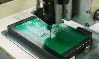
6. Inspection and Testing Methods for Precision PCB Manufacturing
Inspection helps verify whether a finished PCB meets its design specifications. Different inspection methods are used for different accuracy requirements.
6.1 Automated Optical Inspection (AOI)
AOI systems use cameras and image-processing technology to inspect copper patterns and identify visible defects.
Common inspection targets include:
- Open circuits and short circuits
- Trace width deviations
- Copper pattern defects
- Missing or excessive copper
- Pattern alignment issues
AOI is particularly useful for inspecting circuit patterns, although it does not replace all electrical or dimensional tests.
6.2 X-Ray Inspection
X-ray inspection can reveal internal structures that are not visible from the PCB surface. It is useful for evaluating multilayer registration, internal via structures, and certain internal defects.
The inspection method and resolution should be selected according to the board structure and the defects that need to be detected.
6.3 Electrical Testing
Electrical testing verifies whether conductive paths meet specified connectivity requirements.
Common methods include:
- Flying probe testing
- Fixture-based testing
- Continuity testing
- Isolation testing
These methods help identify open circuits and unintended electrical connections. However, electrical testing alone cannot confirm every dimensional or material characteristic.
6.4 Dimensional and Cross-Section Inspection
Dimensional inspection checks board size, thickness, hole position, and other mechanical features against the engineering drawing.
Microsection analysis can be used to examine internal structures, including plated hole walls, copper thickness, and layer construction.
Combining optical, electrical, dimensional, and cross-section inspection provides a more complete evaluation of PCB manufacturing quality.
7. How to Evaluate a Precision PCB Manufacturing Supplier
Choosing a PCB supplier involves more than comparing unit prices. Buyers should determine whether the manufacturer’s actual process capabilities match the design requirements.
Consider the following factors during supplier evaluation:
1. Trace width and spacing capability
Ask about the manufacturer’s minimum trace width and spacing for the required copper thickness and board structure. Confirm that these values apply to production conditions, not only prototype samples.
2. Drilling and via capabilities
Review the supplier’s mechanical drilling, laser drilling, finished hole diameter, and aspect ratio capabilities. Check whether the supplier can support the required PTH, blind via, or buried via structures.
3. Multilayer registration control
For multilayer designs, ask how the supplier manages material expansion, inner-layer compensation, tooling, and lamination alignment.
4. Dimensional inspection procedures
Confirm whether the supplier measures finished board dimensions, thickness, hole positions, and outline geometry according to the agreed drawings.
5. Quality documentation
Discuss inspection records, test reports, material traceability, and applicable quality management certifications. Documentation should match the requirements of the project and the customer’s industry.
6. Engineering communication
A capable supplier should be able to review Gerber files, stack-up requirements, drill files, and fabrication notes before production. Early engineering feedback can help identify tolerance conflicts and reduce manufacturing risks.
8. Conclusion: Precision Comes from Consistent Process Control
Precision PCB manufacturing depends on the combined accuracy of circuit pattern formation, hole drilling, layer registration, and dimensional processing. These factors are closely connected: a deviation in one stage can affect the performance or assembly compatibility of the finished board.
For PCB buyers, the most effective approach is to define measurable tolerances, provide complete design documentation, and evaluate suppliers according to their actual process capabilities and inspection methods. Not every PCB requires the tightest possible tolerances. The goal is to achieve the accuracy needed for the product’s electrical, mechanical, and assembly requirements while maintaining practical manufacturing efficiency.
By understanding these key factors, procurement teams and engineering designers can make better decisions when sourcing custom PCBs. STG supports custom PCB manufacturing requirements through engineering communication and production coordination. Contact our team to discuss your board specifications, stack-up design, and manufacturing requirements.